Assemble (Solder)
Bill of Materials
Introduction
Once the PCB (printed circuit board) and electrical components have been obtained, the components can be soldered onto the board. Orientation of these components is important, and will be explained below.
Step 1: Placing Parts
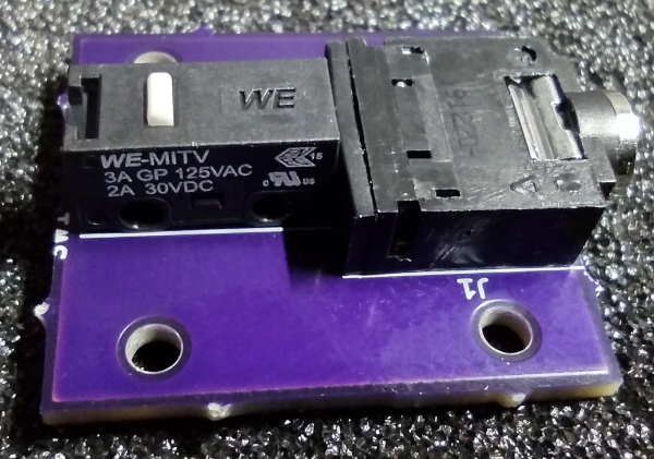
Arrange the components on the PCB in the orientation shown in the following image. Notice that the components are placed on the side of the PCB with the silkscreen (white lines and lettering). This will be considered the top side of the PCB from here out, and it is important to place the components on this side of the PCB.
Notes on Audio Connector Placement
Notice that the barrel connector opening on the audio connector hangs over the edge of the board. The audio connector has pegs on the bottom that should fit closely into the non-plated through holes on the PCB. The audio connector should not fit correctly in any other orientation than that shown in the picture. The collar on the barrel of the connector should just slip past the edge of the PCB so that the connector's bottom is flush with the surface of the board. However, there is a minor design flaw with the current PCB that may cause the barrel of the audio connector to interfere with the edge of the board. This prevents the body of the audio connector from laying flush. If the audio connector looks like the following image, than the connector is interfering with the edge of the PCB.
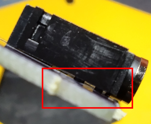
It is best if the audio connector body is flush with the surface of the PCB so that the collar can take some of the pressure off of the solder joints when the user is plugging in an audio connector. However, the solder joints should be strong enough to hold the connector in place under normal use conditions.
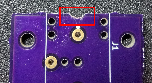
If the audio connector's barrel is interfering and you want to prevent that, you can file a notch in the board directly below the barrel connector. The notch only needs to be 1 millimeter deep and 3 millimeters wide, so be careful not to make it excessively deep, or damage the solder mask, traces, or pads on the board.
This design flaw will be fixed in later revisions.
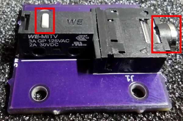
Notes on Microswitch Placement
The plunger of the microswitch, which is the part that gets pressed so that the switch activates, must be oriented as shown in the image at the top of the documentation. The microswitch has two modes of operation. The first is normally open (NO), where the microswitch will not activate and let current flow until the plunger is pushed down. The second is normally closed (NC), where the microswitch will be activated (let current flow) until the plunger is pushed. The push button switch is designed to operate in the normally open configuration, and so the switch must be oriented as shown above so that the correct pins are connected. If the microswitch is turned 180 degrees, the switch will not operate properly. The incorrect orientation will also put the plunger in the wrong position to be depressed by the stem of the switch when the cap is pressed down.
Step 2: Secure the Components to the PCB
The components will likely fall out if the PCB is flipped for soldering without securing them first. This can be done using a piece of tape placed over the component (never between it and the circuit board) on the top side of the board. Masking tape is likely the best type of tape to use for this purpose. Try to get the components as square (aligned) with the edge of the PCB as possible when securing them.
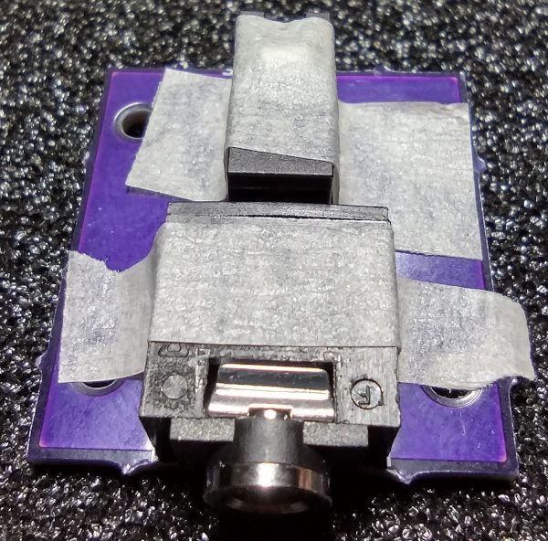
A small amount of hot glue can also be used to hold the components in place, but caution must be used to keep from overheating and melting the parts. It is also important not to use something permanent like super glue.
If many of these boards need to be assembled over time, it may be worth investing in a PCB assembly frame like this one or, better yet, building your own such as this 3D printed one or this aluminum extrusion unit.
Step 3: Flip the PCB and Solder
Once the components have been secured, it is time to flip the board over and use a pencil Soldering Iron and solder the terminals to the pads on the circuit board. The following image shows which pins need to be soldered.
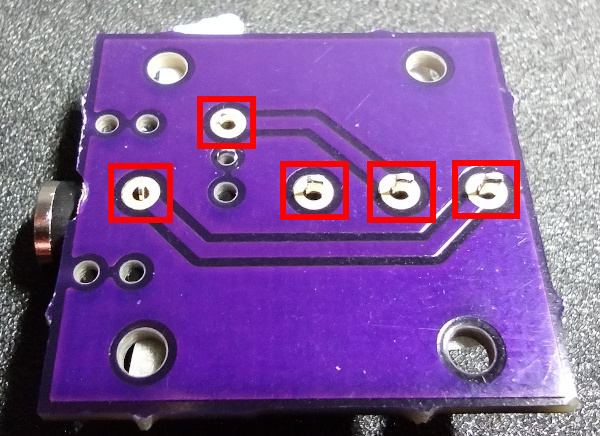
Be sure to create good solder joints (no cold solder joints) without an excess of solder. Once all pins have been soldered, the masking tape can be removed.
If you are new to soldering, there are guides to soldering that can be used as a reference. One example is Adafruit's guide on making good solder joints, which is part of a larger guide that covers everything a beginner needs to know about soldering.
Step 4: Inspect the Assembled Board
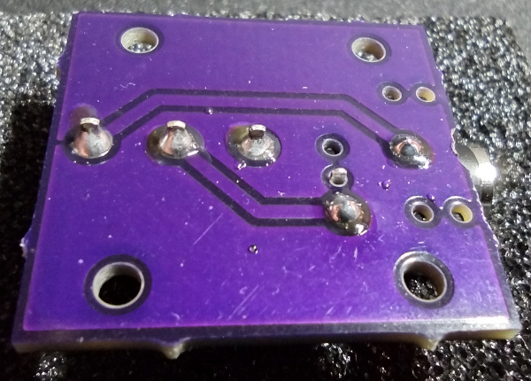
Once the board is soldered, the assembly is complete. Take a moment of inspect the solder joints for any problems, and look at the top side of the board to make sure that the plastic housings of components did not get melted at all and were not bumped out of position during soldering.
The finished board should look something like this.
Step 5: (Optional) Do Continuity Check
Once the circuit board is complete, and if you have a digital multimeter (DMM), a mono audio cable can be plugged into the PCB for testing.
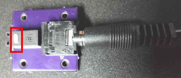
The plunger is highlighted in the previous picture because it can be pressed to close the switch for the test once the DMM is connected.
A DMM can be connected to the two terminals shown below. One on the tip, and one on the sleeve.You are just checking continuity, so the polarity will not matter.
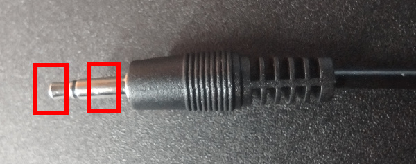
Set the DMM to the continuity check setting and then press the plunger on the microswitch, which is highlighted in the first image in this section. If the DMM shows continuity, the electrical assembly is working correctly.