
Electrical - Push Button Switch Documentation
Contents
In order to complete the electrical portion of the push button switch design, a PCB (Printed Circuit Board) must be made or ordered, the electrical components that go on the PCB must be obtained, and then the components must be soldered onto the PCB. The sections below explain each of these steps, and the steps can be accessed quickly from the content menu above.
PCB Manufacture
The Printed Circuit Board (PCB) for the switch must be manufactured before the switch can be assembled and used in its default configuration. This is normally done by sending the manufacturing files to a vendor, such as OSHPark and then waiting for the finished boards to be shipped. Vendors normally require an account to be created on their website, and then a user can log in and upload the design files and order boards. It can take between 1 week and multiple months to receive a PCB order, depending on the vendor and how busy they are.
The electrical manufacturing files for this project are contained within the project download file here. Extract the nested zip file called "pb_switch_grb.zip" , which contains the manufacturing files. These files are known to work with OSHPark's service, but they will likely work with other services too.
Isolation Routing (Optional Advanced DIY Manufacturing)The PCB has been laid out in such a way that it is possible to use isolation routing on a CNC machine to manufacture it. That is how the initial prototypes were made by 7B Industries. This method should not be attempted unless the user is familiar with CNC machines. This method only provides a board with the proper traces, and does not include solder mask or silkscreen.
When isolation routing is attempted, use a v-shaped engraving bit set to the appropriate depth. The "appropriate depth" will vary based on the exact bit used and the copper thickness on the copper clad board. The traces have 0.508 mm of clearance around them, so by setting the proper depth of the bit and the width of the tool to 0.508 mm, it should be possible to route the board in a single pass. Experimentation is often needed to complete this process effectively though, and is attempted at your own risk.
Order Components
There are three off-the-shelf components that must be obtained in order to fully assemble the circuit board. Each item in the list below has a link of a sample location to purchase it from. However, there are alternate sources for the components.
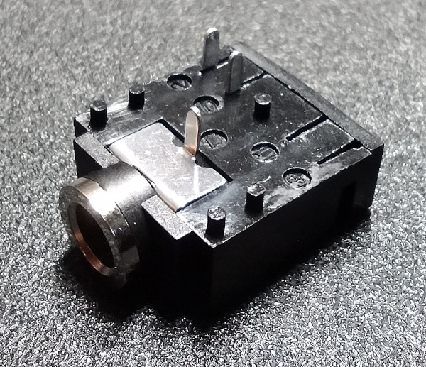
- Audio jack - Adapts the microswitch to work with typical switch interfaces.
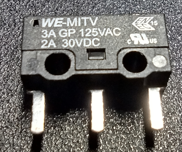
- Microswitch - Switch that determines when a user is pressing down on the button.
- Mono audio cable - Attaches the push button switch to a switch interface. Almost any mono audio cable should work as a substitute.
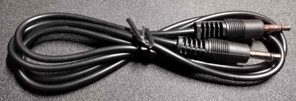
If only a single board is being assembled, one of each part is all that is needed. The audio cable can be purchased in any length that is needed for the application.
Assemble (Solder)
Once the PCB (printed circuit board) and electrical components have been obtained, the components can be soldered onto the board. Orientation of these components is important, and will be explained below.
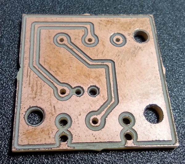
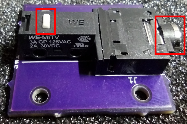
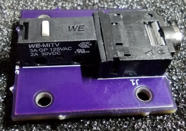
Step 1: Placing PartsArrange the components on the PCB in the orientation shown in the following image. Notice that the components are placed on the side of the PCB with the silkscreen (white lines and lettering). This will be considered the top side of the PCB from here out, and it is important to place the components on this side of the PCB.
Notes on Audio Connector Placement
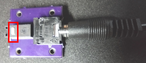
Notice that the barrel connector opening on the audio connector hangs over the edge of the board. The audio connector has pegs on the bottom that should fit closely into the non-plated through holes on the PCB. The audio connector should not fit correctly in any other orientation than that shown in the picture. The collar on the barrel of the connector should just slip past the edge of the PCB so that the connector's bottom is flush with the surface of the board. However, there is a minor design flaw with the current PCB that may cause the barrel of the audio connector to interfere with the edge of the board. This prevents the body of the audio connector from laying flush. If the audio connector looks like the following image, then the connector is interfering with the edge of the PCB.
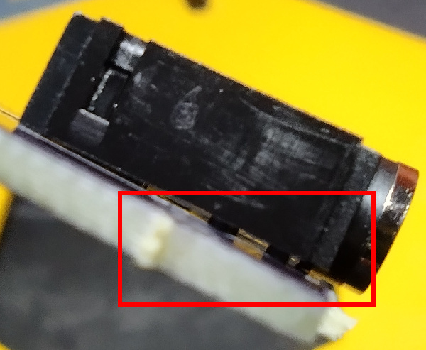
It is best if the audio connector body is flush with the surface of the PCB so that the collar can take some of the pressure off of the solder joints when the user is plugging in an audio connector. However, the solder joints should be strong enough to hold the connector in place under normal use conditions.
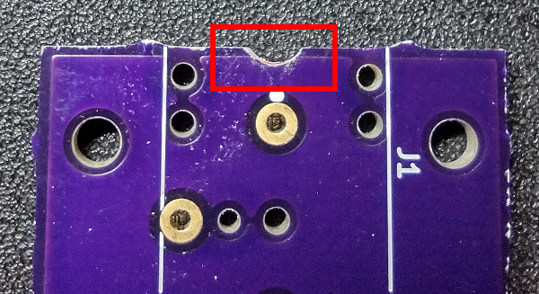
If the audio connector's barrel is interfering and you want to prevent that, you can file a notch in the board directly below the barrel connector. The notch only needs to be 1 millimeter deep and 3 millimeters wide, so be careful not to make it excessively deep, or damage the solder mask, traces, or pads on the board.
This design flaw will be fixed in later revisions.
Notes on Microswitch PlacementThe plunger of the microswitch, which is the part that gets pressed so that the switch activates, must be oriented as shown in the following image.
The microswitch has two modes of operation. The first is normally open (NO), where the microswitch will not activate and let current flow until the plunger is pushed down. The second is normally closed (NC), where the microswitch will be activated (let current flow) until the plunger is pushed. The push button switch is designed to operate in the normally open configuration, and so the switch must be oriented as shown above so that the correct pins are connected. If the microswitch is turned 180 degrees, the switch will not operate properly. The incorrect orientation will also put the plunger in the wrong position to be depressed by the stem of the switch when the cap is pressed down.
Step 2: Secure the Components to the PCB
The components will likely fall out if the PCB is flipped for soldering without securing them first. This can be done using a piece of tape placed over the component (never between it and the circuit board) on the top side of the board. Masking tape is likely the best type of tape to use for this purpose. Try to get the components as square (aligned) with the edge of the PCB as possible when securing them.
A small amount of hot glue can also be used to hold the components in place, but caution must be used to keep from overheating and melting the parts. It is also important not to use something permanent like super glue.
If many of these boards need to be assembled over time, it may be worth investing in a PCB assembly frame like this one or, better yet, building your own such as this 3D printed one or this aluminum extrusion unit.
Step 3: Flip the PCB and SolderOnce the components have been secured, it is time to flip the board over and use a soldering iron to solder the terminals to the pads on the circuit board. The following image shows which pins need to be soldered.
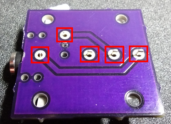
Be sure to create good solder joints (no cold solder joints) without an excess of solder. Once all pins have been soldered, the masking tape can be removed.
If you are new to soldering, there are guides to soldering that can be used as a reference. One example is Adafruit's guide on making good solder joints, which is part of a larger guide that covers everything a beginner needs to know about soldering.
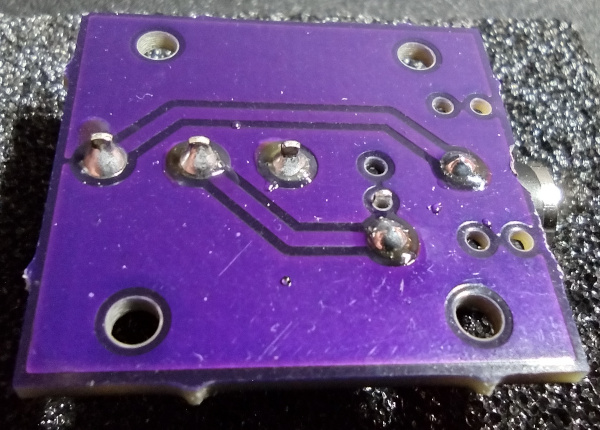
Step 4: Inspect the Assembled BoardOnce the board is soldered, the assembly is complete. Take a moment to inspect the solder joints for any problems, and look at the top side of the board to make sure that the plastic housings of components did not get melted at all, and were not bumped out of position during soldering.
The finished board should look something like these images.
Step 5: (Optional/Recommended) Do a Continuity Check
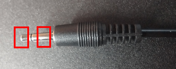
Once the circuit board is complete, and if you have a digital multimeter (DMM) which can check continuity, a mono audio cable can be plugged into the PCB for testing.
The plunger is highlighted in the previous picture because it can be pressed to close the switch for the test once the DMM is connected.
A DMM can be connected to the two terminals shown below. One on the tip, and one on the sleeve. You are just checking continuity, so the polarity will not matter.
Set the DMM to the continuity check setting and then press the plunger on the microswitch. If the DMM shows continuity, the electrical assembly is working correctly.
© 2018-2026 7B Industries